- 您现在的位置:买卖IC网 > Sheet目录477 > MICRF501BLQ TR (Micrel Inc)TXRX SGL 300-600MHZ 44-LQFP
�� �
�
�Radio frequency f� RF�
�Comparison� frequency� f� C�
�VCO� gain� K� o�
�MICRF501�
�Modulation� Inside� PLL�
�A� fast� PLL� requires� a� loop� filter� with� relatively� high� bandwidth.�
�If� a� second� order� loop� filter� is� chosen,� it� may� not� give�
�adequate� attenuation� of� the� comparison� frequency.� There-�
�fore� in� the� following� example� a� third� order� loop� filter� is� chosen.�
�Example� 1:�
�434MHz�
�100kHz�
�Loop� bandwidth� BW� 4.3kHz�
�28MHz/V�
�Phase� comparator� gain� K� d� 500� μ� A/rad�
�Phase� margin� j� 62� °�
�Breakthrough� suppression� A� 20dB�
�The� component� values� will� be:�
�Micrel�
�Data� rates� above� approximately� 19200baud� (including�
�Manchester� encoding)� can� be� used� with� this� loop� filter� without�
�significant� tracking� of� the� modulating� signal.� PLL� lock� time� will�
�be� approximately� 4ms.�
�If� a� faster� PLL� lock� time� is� wanted,� the� charge� pump� can� be�
�made� to� deliver� a� current� of� 500� μ� A� per� unit� phase� error,� while�
�an� open� drain� NMOS� on� chip� (Pin� 10,� CmpR)� switches� in� a�
�second� damping� resistor� (R10)� to� ground� as� shown� in� Figure�
�6.� Once� locked� on� the� correct� frequency,� the� PLL� automati-�
�cally� returns� to� standard� low� noise� operation� (charge� pump�
�current:� 125� μ� A/rad).� If� correct� settings� have� been� made� in� the�
�control� word� (cpmp1� =� 1,� cpmp0� =� 0),� the� fast� locking� feature�
�is� activated� and� will� reduce� PLL� lock� time� by� a� factor� of� two�
�without� affecting� the� phase� margin� in� the� loop.�
�Components� C17,� C18� C19,� R11,� R12,� R13� and� R16� (see�
�IN�
�C115�
�1.5n�
�R101�
�C116�
�33n�
�R109�
�22k�
�C103�
�150p�
�OUT�
�application� circuit)� are� necessary� if� FSK� modulation� is� ap-�
�plied� to� the� VCO.� Data� entered� at� the� DATAIXO-pin� will� then�
�be� fed� through� the� Mod-pin� (Pin� 11)� which� is� a� current� output.�
�The� pin� sources� a� current� of� 50� μ� A� when� Logic� 1� is� entered� at�
�the� DATAIXO� and� drains� the� current� for� Logic� 0.� The� capaci-�
�6.2k�
�Figure� 5.� Third� Order� Loop� Filter�
�With� this� loop� filter,� internal� modulation� up� to� 2400bps� is�
�possible.� The� PLL� lock� time� from� power-down� to� Rx� will� be�
�approximately� 1ms.�
�Modulation� Outside� PLL� (Closed� Loop)�
�When� modulation� is� applied� outside� the� PLL,� it� means� that� the�
�PLL� should� not� track� the� changes� in� the� loop� due� to� the�
�modulation� signal.� A� loop� filter� with� relatively� low� bandwidth�
�is� therefore� necessary.� The� exact� bandwidth� will� depend� on�
�the� actual� modulation� rate.� Because� the� loop� bandwidth� will�
�be� significantly� lower� than� the� comparison� frequency,� a�
�second� order� loop� filter� will� normally� give� adequate� attenua-�
�tion� of� the� comparison� frequency.� If� not,� a� third� order� loop� filter�
�may� give� the� extra� attenuation� needed.�
�Example� 2:�
�tance� of� C17� will� set� the� order� of� filtering� of� the� baseband�
�signal.� A� large� capacitance� will� give� a� slow� ramp-up� and�
�therefore� a� high� order� of� filtering� of� the� baseband� signal,� while�
�a� small� capacitance� gives� a� fast� ramp-up,� which� in� turn� also�
�gives� a� broader� frequency� spectrum.� Resistors� R11� and� R12�
�set� the� frequency� deviation.� If� C18� is� large� compared� to� C17,�
�the� frequency� deviation� will� be� large.� R13� should� be� large� to�
�avoid� influencing� the� loop� filter.� Pin� DATAIXO� must� be� kept�
�in� tri-state� from� the� time� Tx-mode� is� entered� until� one� starts�
�sending� data.�
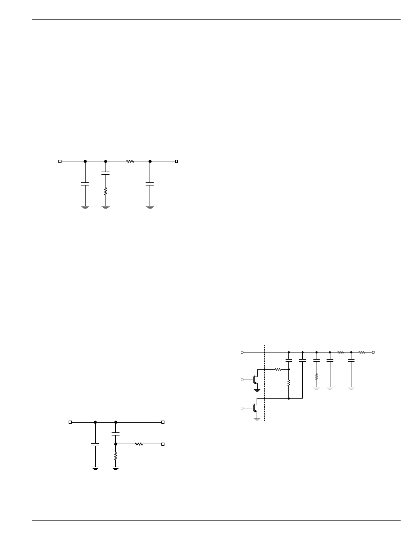
�Modulation� Outside� PLL,� Dual-Loop� Filters�
�Modulation� outside� the� PLL� requires� a� loop� filter� with� a�
�relatively� low� bandwidth� compared� to� the� modulation� rate.�
�This� results� in� a� relatively� long� loop� lock� time.� In� applications�
�where� modulation� is� applied� to� the� VCO,� but� at� the� same� time�
�a� short� start-up� time� from� power� down� to� receive� mode� is�
�needed,� dual-loop� filters� can� be� implemented.� Figure� 7�
�shows� how� to� implement� dual-loop� filters.�
�Radio� frequency� f� RF�
�Comparison� frequency� f� C�
�434MHz�
�140kHz�
�Loop� bandwidth� BW� 1.03kHz�
�CMPOUT�
�Pin9�
�Pin10�
�C16�
�100n�
�R10�
�C15�
�6.8n�
�C116�
�33n�
�R109�
�C115�
�1.5n�
�R102� 22k�
�C103�
�150p�
�R8� 47k�
�towards_VCO�
�VCO� gain� K� o�
�Phase� comparator� gain� K� d�
�Phase� margin� j�
�The� component� values� will� be:�
�28MHz/V�
�125� μ� A/rad�
�62� °�
�FLC�
�DFC�
�Pin4�
�6.2k�
�R9�
�6.2k�
�6.2k�
�IN�
�C16�
�OUT�
�Figure� 7.� Dual-Loop� Filters�
�C15�
�6.8n�
�100n�
�R9�
�8.2k�
�R10�
�8.2k�
�CmpR�
�The� loop� filter� used� in� transmit� mode� is� made� up� of� C15,� C16,�
�R9� and� R10.� The� fast� lock� feature� is� also� included� (internal�
�NMOS� controlled� by� FLC,� Fast� Lock� Control).� This� filter� is�
�automatically� switched� in/out� by� an� internal� NMOS� at� Pin� 4,�
�Figure� 6.� Second� Order� Loop� Filter�
�QchOut,� which� is� controlled� by� DFC� (Dual� Filter� Control).� Bits�
�OutS2,� OutS1,� OutS0� must� be� set� to� 110.� When� QchOut� is�
�used� to� switch� the� Tx� loop� filter� to� ground,� neither� QchOut� nor�
�IchOut� can� be� used� as� test� pins� to� look� at� the� different� receiver�
�March� 2003�
�11�
�MICRF501�
�发布紧急采购,3分钟左右您将得到回复。
相关PDF资料
MICRF505DEV1
KIT DEV RADIOWIRE 850-950MHZ
MICRF506DEV1
EVAL BOARD EXPERIMENTAL MICRF506
MICRF507YML TR
TXRX FSK LOW PWR W/AMP 32MLF
MICRF600DEV1
KIT DEV RADIOWIRE 902-928MHZ
MK01-C
SENSOR REED SPST-NO SMD
MK01-H
SENSOR REED SPDT-CHANGE SMD
MK02/0-1A66-500W
SENSOR REED SPST-NO
MK02/6-0
SENSOR REED PCB 24MM T/H
相关代理商/技术参数
MICRF501EVAL1
功能描述:EVAL BOARD EXPERIMENTAL MICRF501 RoHS:否 类别:RF/IF 和 RFID >> RF 评估和开发套件,板 系列:RadioWire® 标准包装:1 系列:- 类型:GPS 接收器 频率:1575MHz 适用于相关产品:- 已供物品:模块 其它名称:SER3796
MICRF505
制造商:MICREL 制造商全称:Micrel Semiconductor 功能描述:868MHz and 915MHz ISM Band Transceiver
MICRF505_07
制造商:MICREL 制造商全称:Micrel Semiconductor 功能描述:850MHz and 950MHz ISM Band Transceiver
MICRF505BML
制造商:Rochester Electronics LLC 功能描述: 制造商:RF Micro Devices Inc 功能描述:
MICRF505BML TR
功能描述:TXRX ISM 868-915MHZ 32-MLF RoHS:否 类别:RF/IF 和 RFID >> RF 收发器 系列:- 产品培训模块:Lead (SnPb) Finish for COTS
Obsolescence Mitigation Program 标准包装:30 系列:- 频率:4.9GHz ~ 5.9GHz 数据传输率 - 最大:54Mbps 调制或协议:* 应用:* 功率 - 输出:-3dBm 灵敏度:- 电源电压:2.7 V ~ 3.6 V 电流 - 接收:* 电流 - 传输:* 数据接口:PCB,表面贴装 存储容量:- 天线连接器:PCB,表面贴装 工作温度:-25°C ~ 85°C 封装/外壳:68-TQFN 裸露焊盘 包装:管件
MICRF505DEV1
功能描述:射频开发工具 MICRF505 Evaluation Kit - For experimental use only
RoHS:否 制造商:Taiyo Yuden 产品:Wireless Modules 类型:Wireless Audio 工具用于评估:WYSAAVDX7 频率: 工作电源电压:3.4 V to 5.5 V
MICRF505DEV1
制造商:Micrel Inc 功能描述:KIT MICRF505 EVALUATION
MICRF505L
制造商:MICREL 制造商全称:Micrel Semiconductor 功能描述:850MHz and 950MHz ISM Band Transceiver